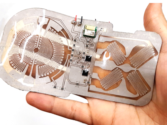
To address this problem, researchers from the University of Coimbra (UC) have developed and tested a new architecture of materials and fabrication techniques that allow us to reverse this reality and apply a new version of 3Rs policy (reduce, reuse and recycle) in the electronics area. That is 3R electronics (resilient, repairable, and recyclable). The results were published in the journal Advanced Materials.
"The research, funded under the scope of CMU Portugal project WoW, represents a breakthrough toward overcoming technological pollution. Currently, the production of electronic waste has reached an alarming level of 7 kg/person/year. Only 20 percent of e-waste is sent for recycling, and only a small percentage of precious metals, mainly gold, are recovered", according to a statement .
Mahmoud Tavakoli, the lead author of the scientific article, explains that soft electronics based on novel polymers will be the best response to the problem of the e-waste. But despite the advances in soft electronics, the 3R electronics is only possible “if we can demonstrate new manufacturing techniques that, on the one hand, are based on resilient, repairable and recyclable materials and, on the other hand, can compete with existing PCB manufacturing techniques in terms of patterning resolution, multi-layer implementation, microchip integration and autonomous manufacturing”.
This research work, which is being carried out at the Institute of Systems and Robotics (ISR) of the Department of Electrical and Computer Engineering (DEEC) of the University of Coimbra, introduces a new architecture for scalable, autonomous, and high-resolution production of 3R electronic devices.
According to Mahmoud Tavakoli, ISR researcher and professor at UC, another differentiating factor is that the manufacturing process is entirely performed at room temperature, an essential step for green electronics: “everything is done at room temperature, including the deposition, patterning, and microchip soldering. Eliminating the temperature from the sintering process (as is common in printed electronics) and from the soldering process considerably reduces energy consumption, and is a step toward the use of green polymers, that were not possible before due to their heat sensitivity”.
"This research presents a paradigm shift toward a more sustainable future and provides the foundation for the next generation of recyclable electronic devices. The team has shown the application of this architecture for wireless biomonitoring patches, and smart textiles that integrate state of the art microchips, for monitoring body temperature, electrocardiogram, respiration frequency, and detection of human motions such as swallowing, or classification of sport activities through wearable sensors", it reads a note.
However, when it comes to industrial level PCBs, such as the ones we see in mobile phones, these developed techniques still require further technological development “to reach the same maturity as the current printed circuit technology. We are rapidly making steps toward industrial-level maturity. We hope in less than 5 years we can start the process for substitution of some the current electronics circuits”, concludes Mahmoud Tavakoli.


